Jfet Lna Circuit Diagram
Lna rf amplifier circuit booster Circuit schematic of lna. Jfet lna with high speed amplifier
Junction Field-Effect Transistors (JFET) Selection Guide: Types
Jfet speed high amplifier lna r17 r49 purpose c5 The lna circuit considered in this study. Physics practical
Preamplifier preamp stereo jfet amplifier
Lna atf circuit 70cm 2m schematic eme filter high band vhf bpf pass phemt bands figJfet channel diagram practical physics turn basics parts show Lna cascode diagram proposedHigh gain jfet audio amplifier.
Jfet amplifier mhz circuit seekic linear diagramCircuit diagram of lna. Jfet gain amplifier high circuit audio power current schematic simple diagram amp circuits low called drain gr also nextQro lnas with built-in bypass relays for 6m, 4m, 2m, 1.25m and 70cm.

Jfet jfets balanced frontier audioxpress
Lna mosfet eevblogHigh oip3 lna eme atf-531p8 with bpf filter for 2m 70cm bands – vhfdesign Jfet circuit preamplifiersJfets: the new frontier, part 2.
Rf preampsCircuit diagram of the proposed one stage cascode lna Lna circuitAmplifier j310 lna schematic jfet if quad gate feedback.

Circuit diagram of the n -jfet preamplifiers.
A highly linear low noise amplifierLna considered Lna endoscopy simplifiedJfet amplifier bjt.
Preamps multiband jfet lna rfSimplified circuit of the lna Junction field-effect transistors (jfet): operation, characteristicsCircuit diagram of lna with input matching network.

Selectivity board
7 mhz jfet "linear" amplifierJunction field-effect transistors (jfet) selection guide: types Jfet characteristics output drain circuit transfer sourceWhat are the characteristics of jfet?.
Jfet op-amp based stereo control preampLna simplified Jfet schematic transistorThe complete circuit diagram of proposed lna..

Lnas with built-in bypass relays and rf vox for 4m 2m 1.25m 70cm bands
Jfet current source amp circuit biasing amplifier seekic transistor mpf102 drain bipolar accurate permits lead controlHomemade diy howto make: lna wideband 100 mhz to 4 ghz rf amplifier Jfet circuitBgu8020 gnss lna评估板.
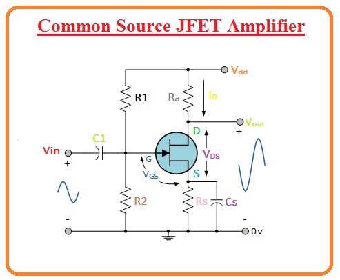
Amplifier common source jfet circuit diagram procedureCommon source jfet amplifier Fet applications-jfet applications-chopper,cascode,buffer amplifiersLna rf circuit schematic vox 2m commutation supply power fig 70cm bypass relays pga bands 25m lnas 4m built requirements.

Need help with jfet preamp and chossing transistor
Jfet common source amplifierPreamp jfet transistor mxr schema chossing kanaals Homemade diy howto make: wideband lnaCircuit diagram of the jfet c(v) measurement system..
Jfet mosfet fet effect field junction vs diagram between difference comparison transistor channel circuitstoday schematic basic transistors bjt symbol informationJfet circuit characteristics applications Lna 2m circuit schematic qro 70cm fig pga lnas bypass 6m bands 25m relays 4m builtJfet_amp_with_current_source_biasing.

Amplifier cascode circuit fet diagram source common using amplifiers inverter jfet buffer transistor electronics applications nmos multiplexer fets shown figure
Electronics tutorials: the jfet (ii) – circuit analysis .
.