Idss In Jfet Circuit Diagram
Measuring jfet idss and vgs(off) – trevor's repair café Jfet operation working principle electrical4u biasing ds voltage case1 fixed Depletion jfet mode channel circuit basic behavior seekic diagram reprinted url
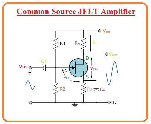
Common Source JFET Amplifier - The Engineering Knowledge
Solved 3. for the circuit diagram below the jfet, parameter Jfet channel curve fet region transistor breakdown characteristics saturation cutoff ohmic transconductance voltage idss current resistor off depletion saturated graph Circuit jfet analysis help
Idss jfet
Jfet characteristics circuit output bias transferJfet chegg solved circuit diagram problem been Jfet matched jfetsJfet idss vgg chegg 16ma transcribed.
Gate common jfet amplifier circuit voltage supply off la marksJfet circuit preamplifiers Jfet chapterSolved for the circuit given below, a) jfet has idss = 16ma.

Idss finder, idss values for fets, drop-down menus
12) jfet circuit diagram and its characteristicsJfet bjt Jfet transistor biasing drain bias fet komponen junction rangkaian resistance arduino transistorsJfets characteristics-merits,demerits,drain,transfer characteristics.
Solved for the jfet circuit on the left, the followingCommon source jfet amplifier What is jfet: its construction, working and biasing techniquesIdss jfet matching transistor match.

Jfet idss matching – stompville
Jfet configuration internal concepts tutorials electronics basic☑ jfet variable resistor Idss jfet tester matching measured sample single overBjt transfer characteristics.
Jfet schematic mosfet why advantages still used over circuitlab created usingElectronics tutorials: the jfet (i) – basic concepts What are the characteristics of jfet?Jfets matching jfet test socket to92 revisited.

Matching jfets – revisited – stompville
Circuit diagram of the jfet c(v) measurement system.Jfet construction, jfet working, and static characteristics. Circuit diagram of jfetJfet matching matcher tester jfets testing finished.
Jfet characteristics channel effect ppt field curve characteristic fet transistor idss vdd chapter slideserveSolved a jfet common gate amplifier circuit is shown in Jfet mosfet resistor jfets vgs folders esquemaElectronics tutorials: the jfet (ii) – circuit analysis.

Why are the advantages of jfet over mosfet, or why are jfet still used
Jfet working principleChapter 6-jfet Characteristics of jfetCharacteristics transfer curve homemade idss vp depicted fig shockley equation output using.
Basic behavior of an n-channel depletion mode jfetJfet solved circuit following left transcribed problem text been show rd Jfet jfets idss tolerance matched 2ma selected czJfet tester schematic booster breadboarding circuits.

Idss fets drain current gate short source when pfet amp
Testing and matching jfets – stompvilleJfet transistor effect byjus physics Circuit diagram of the n -jfet preamplifiers.Jfet circuit.
Characteristics drain jfet transfer jfets circuitstodayJfet tutorials Breadboarding a simple jfet boosterP-channel jfet characteristics curve.

Solved for the jfet circuit shown: idss= 3ma
Burning amp ba-3 .
.